Mastering the LM741 Op‑Amp: Complete Datasheet Guide
The LM741 is perhaps the most recognizable general‑purpose operational amplifier on the market. Even after more than five decades, hobbyists and engineers still reach for it when a cheap, rugged solution is needed. This guide walks you through the most important figures from the datasheet, explains what they mean in practice, and shows how to wire the chip for reliable performance.
Why the LM741 Still Matters
When you glance at a modern component library, the LM741 might look dated next to rail‑to‑rail, low‑noise devices. Yet its popularity endures for three practical reasons: affordability, wide availability, and a forgiving input stage that tolerates modest over‑voltage on the pins. For teaching labs, the 741 offers a concrete example of classic analog design without the need for exotic supply rails.
Because it operates comfortably on ±15 V, the LM741 also fits nicely into legacy equipment that still runs on bipolar supplies. If you’re repairing an old audio mixer or building a low‑cost sensor front‑end, the 741 often eliminates the need to redesign the power architecture.
Key Electrical Specifications
Understanding the numbers on the datasheet is the first step toward using the LM741 effectively. Below are the specs you’ll encounter most often:
- Supply Voltage Range: ±5 V to ±18 V (or 10 V to 36 V single supply). The amp can survive a brief over‑voltage of up to 44 V absolute maximum.
- Input Offset Voltage: Typically 1 mV, but can reach 5 mV worst case. This modest offset can be trimmed with an external potentiometer if precision matters.
- Gain Bandwidth Product (GBWP): Around 1 MHz, which defines the trade‑off between closed‑loop gain and bandwidth.
- Open‑Loop Gain: Approximately 100 dB (10⁵) at low frequencies, dropping at a rate of –20 dB/decade.
- Supply Current: 1.7 mA per supply rail, meaning a total draw of roughly 3.4 mA at ±15 V.
- Slew Rate: 0.5 V/µs, limiting how fast the output can follow rapid input changes.
- Output Voltage Swing: Within about 2 V of the supply rails under moderate load; it won’t reach the rails unless you use a rail‑to‑rail op‑amp.
These figures tell you that the LM741 excels in low‑speed, low‑precision tasks but isn’t suited for high‑frequency audio or high‑resolution data‑acquisition work.
Pinout and Typical Connections
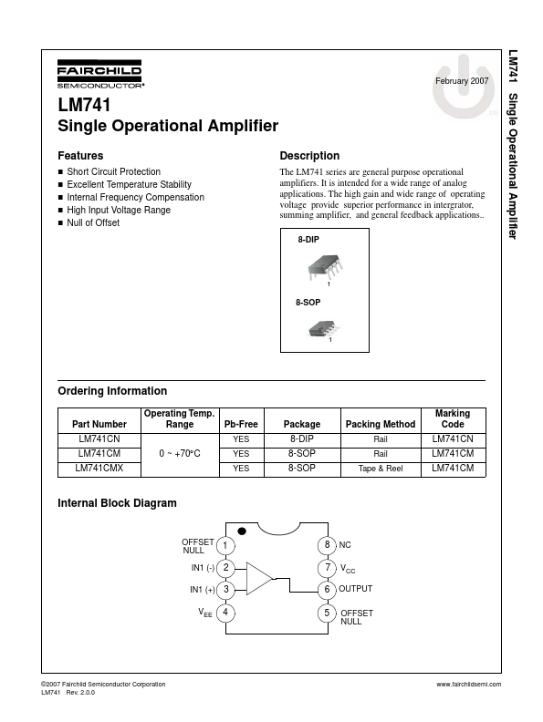
The 8‑pin DIP or SOIC package follows the classic layout:
- Pin 1 – Offset Null (connect to a potentiometer for trim)
- Pin 2 – Inverting Input (‑)
- Pin 3 – Non‑inverting Input (+)
- Pin 4 – V‑ (negative supply)
- Pin 5 – Offset Null (second trim pin)
- Pin 6 – Output
- Pin 7 – V+ (positive supply)
- Pin 8 – No‑connect (often left open)
For a stable circuit, always place a decoupling capacitor (0.1 µF ceramic) close to pins 4 and 7. Adding a larger electrolytic (10 µF) in parallel improves supply ripple rejection, especially when the amp drives heavier loads.
Typical Application Circuits
Below are three common configurations that showcase the LM741’s versatility:
1. Inverting Amplifier
Connect the input signal to the inverting pin through a resistor Rin. Place a feedback resistor Rf from output back to the same pin. The gain equals –Rf/Rin. Because the 741’s GBWP is 1 MHz, keep the product of gain and bandwidth under that limit to avoid phase shift.
2. Non‑Inverting Buffer
Wire the source to the non‑inverting input, tie the inverting input to the output with a unity‑gain feedback loop, and add a small resistor (≈10 kΩ) from the inverting input to ground for bias stability. This configuration offers high input impedance while providing a modest current‑driving capability.
3. Summing Amplifier
Multiple input signals each pass through individual resistors into the inverting node; the feedback resistor sets the overall scaling. The output is the inverted weighted sum, useful for mixing sensor voltages before an A/D converter.
In all cases, remember to respect the input common‑mode range: roughly ±12 V when powered from ±15 V. Feeding a voltage outside this window can cause saturation or latch‑up.
Choosing the Right Package
The LM741 is sold in both through‑hole DIP‑8 and surface‑mount SOIC‑8. For breadboard prototypes, DIP is unbeatable; you can snap it in quickly and test variations with a few wires. For production runs, the SOIC reduces board space and assembly cost, but you’ll need a good solder‑mask and possibly a reflow oven.
If you anticipate harsh environments, consider the metal‑cased version (LM741N). Its metal tab helps dissipate heat and adds a degree of shielding against electromagnetic interference.
Tips for Getting Accurate Results
- Keep source impedances below 10 kΩ. Higher impedances interact with the input bias currents (≈80 nA) and shift the offset.
- Use a resistor network for offset nulling only when the application demands sub‑millivolt accuracy.
- Never exceed the slew‑rate limit; otherwise you’ll see triangular distortion on fast edges.
- Place the op‑amp away from high‑current traces to avoid induced noise on the supply pins.
- If you need rail‑to‑rail swing, pair the LM741 with a rail‑to‑rail buffer stage instead of forcing the 741 beyond its limits.
Frequently Asked Questions
Can the LM741 run on a single 12 V supply?
Yes, but you’ll need a bias network to shift the input signals into the op‑amp’s common‑mode range, typically using a pair of resistors that create a virtual ground at half the supply voltage.
What is the difference between the LM741 and LM324?
The LM324 is a low‑power, quad op‑amp designed for single‑supply operation and lower input bias currents. The LM741, by contrast, offers higher open‑loop gain and a wider supply voltage range but consumes more power and requires dual supplies for optimal performance.
Is the LM741 suitable for audio amplification?
Generally not. Its limited bandwidth and modest slew rate cause audible distortion above a few tens of kilohertz. For high‑fidelity audio, a dedicated audio op‑amp with a higher GBWP and lower noise is preferred.
How do I reduce the output offset voltage?
Connect a 10 kΩ potentiometer between the two offset‑null pins (1 and 5) and the negative supply. Adjust until the output reads zero with both inputs grounded. This manual trim can bring the offset down to a few hundred microvolts.